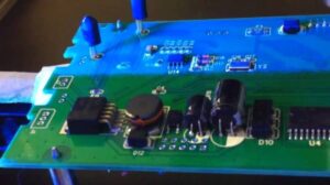
In the intricate world of electronics manufacturing, Printed Circuit Boards (PCBs) are the nervous system of virtually every modern device. From industrial control systems operating in harsh environments to delicate medical equipment, the reliability and longevity of PCBs are paramount. Protecting these vital components from environmental stressors, mechanical shock, and electrical interference is not merely a best practice; it’s a critical differentiator in today’s competitive market. This is where PCB potting compounds play an indispensable role.
This blog post will delve into the transformative power of PCB potting, explore the diverse challenges it addresses, and highlight how Incure delivers cutting-edge PCB potting compounds and expert support to help manufacturers and industry professionals achieve unparalleled product performance and reliability.
Why PCB Potting Compound is Non-Negotiable for Modern Electronics
PCB potting is the process of encapsulating a printed circuit board, or specific electronic components, within a protective material, typically a liquid resin that cures into a solid or gel-like barrier. This seemingly simple step offers a multitude of benefits that directly impact the durability, functionality, and lifespan of electronic devices:
- Environmental Protection: Potting creates an impenetrable barrier against moisture, humidity, dust, dirt, and corrosive chemicals. This is crucial for devices exposed to outdoor elements, industrial pollutants, or even internal condensation.
- Mechanical Protection: The cured potting compound acts as a shock absorber, protecting delicate components and solder joints from vibration, impact, and mechanical stress. This is vital in automotive, aerospace, and portable electronics.
- Electrical Insulation: Potting compounds possess high dielectric strength, preventing electrical arcing, short circuits, and corona discharge, particularly in high-voltage applications. They also help maintain signal integrity.
- Thermal Management: Certain PCB potting compounds are formulated with thermal conductivity, facilitating efficient heat dissipation away from critical components, preventing overheating and extending operational life.
- Tamper Proofing & Security: Encapsulating sensitive circuits makes them resistant to reverse engineering or unauthorized tampering, adding a layer of security for intellectual property.
- Improved Reliability & Longevity: By mitigating the risks mentioned above, PCB potting significantly enhances the overall reliability and extends the operational lifespan of electronic assemblies, reducing warranty claims and maintenance costs.
Without robust protection, PCBs are vulnerable to premature failure, leading to costly downtime, reputational damage, and loss of competitive edge.
The Incure Advantage: Tailored PCB Potting Solutions
Incure understands that one size does not fit all in PCB protection. The ideal PCB potting compound depends heavily on the specific application’s demands, including operating environment, thermal requirements, flexibility needs, and desired curing speed. Incure offers a comprehensive range of PCB potting compounds, each engineered with precise properties to address these diverse needs, alongside unparalleled technical expertise.
Here’s how Incure empowers your projects with superior PCB potting solutions:
1. Diverse Formulations for Every Challenge
Incure’s portfolio includes a variety of advanced PCB potting compounds, ensuring you find the perfect match for your application:
- UV-Curable Potting Compounds: Leveraging the power of UV light, these compounds offer incredibly rapid curing times (seconds to minutes), dramatically accelerating production cycles. Incure’s UV potting compounds are ideal for high-volume manufacturing where speed and precision are paramount. Our Uni-Seal™ series, for instance, includes UV-curable options that provide excellent adhesion and environmental resistance with ultra-low shrinkage.
- Dual-Cure Solutions: For complex PCB geometries with “shadowed areas” where UV light cannot reach, Incure offers innovative dual-cure potting compounds (e.g., UV/thermal or UV/moisture). These compounds initiate curing with UV light and then complete the process with a secondary mechanism, ensuring thorough protection even in hard-to-reach spots.
- Specialized Properties: Whether you require compounds with exceptional thermal conductivity for heat-generating components, superior flexibility for shock absorption, flame retardancy for safety-critical applications, or optically clear formulations for LED assemblies, Incure has a solution. We offer products like Uni-Seal™ 6213HT, an epoxy-acrylate blend designed for high-temperature resistance and low water absorption, crucial for demanding electronics.
2. Expert Application Guidance and Process Optimization
Selecting the right compound is just the beginning. Effective PCB potting requires a meticulous process. Incure’s team of seasoned technical experts provides invaluable support to optimize your entire potting workflow:
- Material Selection Assistance: We work closely with you to analyze your specific requirements – from environmental stressors and temperature ranges to component sensitivity and production throughput – to recommend the most suitable PCB potting compound.
- Dispensing & Curing Integration: Incure offers insights into optimal dispensing techniques (manual or automated) and guides you in integrating the most efficient curing equipment. For UV-curable compounds, this includes advising on appropriate UV lamp types, intensity, and exposure times to ensure a complete and consistent cure.
- Troubleshooting & Process Refinement: From minimizing voids and air bubbles to ensuring perfect adhesion and consistent cure depths, Incure provides hands-on support to refine your potting process, reduce waste, and improve yield. We understand common challenges like thermal expansion mismatch and can help select compounds with compatible Coefficients of Thermal Expansion (CTE).
3. Enhancing Reliability and Cost Efficiency
By partnering with Incure, manufacturers can directly translate advanced material science into tangible business benefits:
- Reduced Product Failures: Superior protection against environmental and mechanical stresses leads to fewer field failures, improving product reputation and customer satisfaction.
- Lower Manufacturing Costs: Rapid curing of UV compounds, reduced rework, and minimized material waste contribute to significant cost savings and increased production efficiency.
- Faster Time-to-Market: Accelerated potting processes allow for quicker product iteration and faster deployment of new devices.
Practical Insights for Optimal PCB Potting
To maximize the effectiveness of PCB potting compounds in your operations, consider these actionable insights:
- Thorough Surface Preparation: Ensure PCBs and components are clean, dry, and free of contaminants (dust, oil, flux residues) to promote optimal adhesion of the potting compound.
- Strategic Dispensing: Employ dispensing techniques that minimize air entrapment. Slow, controlled pouring or automated dispensing with vacuum degassing can significantly reduce voids, which are weak points in the protective layer.
- Controlled Curing Environment: For UV-curable compounds, consistently monitor UV light intensity and wavelength using a radiometer. For thermal-curing compounds, maintain strict control over oven temperature and curing time.
- Consider Reworkability: While potting offers robust protection, it can make rework challenging. If future component replacement or repair is a possibility, discuss this with Incure’s specialists to explore compounds that offer a degree of reworkability, such as softer gel-like silicones or specific polyurethane formulations.
- Prototype and Test Rigorously: Always conduct extensive testing on potted prototypes under simulated real-world conditions (e.g., thermal cycling, humidity exposure, vibration tests) to validate the chosen compound and process.
Partner with Incure for Unrivaled PCB Protection
The demands on electronic devices continue to escalate, requiring robust protection that ensures long-term performance in increasingly challenging environments. PCB potting compounds are a cornerstone of this protection.
Incure stands as your trusted partner, offering not just a portfolio of high-performance PCB potting compounds, but a commitment to deep technical collaboration. We empower individuals and professionals in manufacturing to solve complex protection challenges, enhance product durability, and gain a decisive edge in the market.
Ready to safeguard your electronic innovations with industry-leading PCB potting solutions? Contact Incure today to discover how our expertise can elevate the reliability and longevity of your projects.